GaN Systems Consumer Articles
 https://cn.gansystems.com/wp-content/uploads/2017/03/G_Philos-Silicon-vs-GaN-ESS.jpg
469
490
gaN-admin
https://cn.gansystems.com/wp-content/uploads/2024/03/infineon-formerly-gan-fc.png
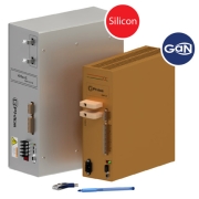
gaN-admin2017-04-26 13:35:572018-02-07 22:24:42Observations about the impact of GaN technology
https://cn.gansystems.com/wp-content/uploads/2017/03/G_Philos-Silicon-vs-GaN-ESS.jpg
469
490
gaN-admin
https://cn.gansystems.com/wp-content/uploads/2024/03/infineon-formerly-gan-fc.png
gaN-admin2017-04-26 13:35:572018-02-07 22:24:42Observations about the impact of GaN technology https://cn.gansystems.com/wp-content/uploads/2017/04/SolPad-PR-banner.png
460
1920
gaN-admin
https://cn.gansystems.com/wp-content/uploads/2024/03/infineon-formerly-gan-fc.png
gaN-admin2017-04-26 08:34:302019-01-28 20:05:46氮化镓系统 (GaN Systems)’ Transistors Enable SolPad’s Revolutionary Solar Power Inverter
https://cn.gansystems.com/wp-content/uploads/2017/04/SolPad-PR-banner.png
460
1920
gaN-admin
https://cn.gansystems.com/wp-content/uploads/2024/03/infineon-formerly-gan-fc.png
gaN-admin2017-04-26 08:34:302019-01-28 20:05:46氮化镓系统 (GaN Systems)’ Transistors Enable SolPad’s Revolutionary Solar Power Inverter https://cn.gansystems.com/wp-content/uploads/2017/04/CPSS-PR-banner.png
460
1920
gaN-admin
https://cn.gansystems.com/wp-content/uploads/2024/03/infineon-formerly-gan-fc.png
gaN-admin2017-04-24 13:51:442018-01-27 23:47:04Designers Compete to Achieve High Power Density Inverters Using GaN Power Transistors
https://cn.gansystems.com/wp-content/uploads/2017/03/G_Philos-Silicon-vs-GaN-ESS.jpg
469
490
gaN-admin
https://cn.gansystems.com/wp-content/uploads/2024/03/infineon-formerly-gan-fc.png
gaN-admin2017-03-20 15:21:192019-01-29 02:26:10GaN Eliminates Fans and Heat Sinks in Power Electronics
https://cn.gansystems.com/wp-content/uploads/2017/04/CPSS-PR-banner.png
460
1920
gaN-admin
https://cn.gansystems.com/wp-content/uploads/2024/03/infineon-formerly-gan-fc.png
gaN-admin2017-04-24 13:51:442018-01-27 23:47:04Designers Compete to Achieve High Power Density Inverters Using GaN Power Transistors
https://cn.gansystems.com/wp-content/uploads/2017/03/G_Philos-Silicon-vs-GaN-ESS.jpg
469
490
gaN-admin
https://cn.gansystems.com/wp-content/uploads/2024/03/infineon-formerly-gan-fc.png
gaN-admin2017-03-20 15:21:192019-01-29 02:26:10GaN Eliminates Fans and Heat Sinks in Power Electronics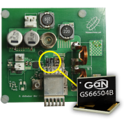 https://cn.gansystems.com/wp-content/uploads/2017/01/Wireless-Charger-with-GaN-Systems-transistors.png
460
500
gaN-admin
https://cn.gansystems.com/wp-content/uploads/2024/03/infineon-formerly-gan-fc.png
gaN-admin2017-03-15 17:35:422018-01-27 23:47:14氮化镓系统 (GaN Systems) Enables Wireless Power Transfer for Laptops, Power Tools and Beyond
https://cn.gansystems.com/wp-content/uploads/2017/01/Wireless-Charger-with-GaN-Systems-transistors.png
460
500
gaN-admin
https://cn.gansystems.com/wp-content/uploads/2024/03/infineon-formerly-gan-fc.png
gaN-admin2017-03-15 17:35:422018-01-27 23:47:14氮化镓系统 (GaN Systems) Enables Wireless Power Transfer for Laptops, Power Tools and Beyond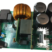 https://cn.gansystems.com/wp-content/uploads/2017/03/APEC-image-PFC-Reference-Design_small.png
357
600
gaN-admin
https://cn.gansystems.com/wp-content/uploads/2024/03/infineon-formerly-gan-fc.png
gaN-admin2017-03-13 17:42:462018-01-27 23:47:14GaN Modules and Solutions are on Display at Electronica Shanghai 2017
https://cn.gansystems.com/wp-content/uploads/2017/03/APEC-image-PFC-Reference-Design_small.png
357
600
gaN-admin
https://cn.gansystems.com/wp-content/uploads/2024/03/infineon-formerly-gan-fc.png
gaN-admin2017-03-06 15:09:152018-01-27 23:47:14GaN Customer Solutions to Take Center Stage at APEC 2017
https://cn.gansystems.com/wp-content/uploads/2017/03/APEC-image-PFC-Reference-Design_small.png
357
600
gaN-admin
https://cn.gansystems.com/wp-content/uploads/2024/03/infineon-formerly-gan-fc.png
gaN-admin2017-03-13 17:42:462018-01-27 23:47:14GaN Modules and Solutions are on Display at Electronica Shanghai 2017
https://cn.gansystems.com/wp-content/uploads/2017/03/APEC-image-PFC-Reference-Design_small.png
357
600
gaN-admin
https://cn.gansystems.com/wp-content/uploads/2024/03/infineon-formerly-gan-fc.png
gaN-admin2017-03-06 15:09:152018-01-27 23:47:14GaN Customer Solutions to Take Center Stage at APEC 2017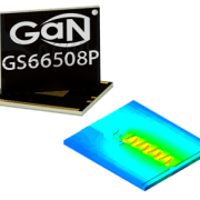 https://cn.gansystems.com/wp-content/uploads/2017/02/GS66508P-thermal-image_2.png
286
360
gaN-admin
https://cn.gansystems.com/wp-content/uploads/2024/03/infineon-formerly-gan-fc.png
gaN-admin2017-02-03 06:34:522018-01-27 23:47:14Thermal Models of 氮化镓系统 (GaN Systems)’ Industry-leading GaN Transistors Now on the Web
https://cn.gansystems.com/wp-content/uploads/2017/01/Wireless-Charger-with-GaN-Systems-transistors.png
460
500
gaN-admin
https://cn.gansystems.com/wp-content/uploads/2024/03/infineon-formerly-gan-fc.png
gaN-admin2017-01-16 14:02:442018-01-27 23:47:14AirFuel Alliance adds 氮化镓系统 (GaN Systems)
https://cn.gansystems.com/wp-content/uploads/2017/02/GS66508P-thermal-image_2.png
286
360
gaN-admin
https://cn.gansystems.com/wp-content/uploads/2024/03/infineon-formerly-gan-fc.png
gaN-admin2017-02-03 06:34:522018-01-27 23:47:14Thermal Models of 氮化镓系统 (GaN Systems)’ Industry-leading GaN Transistors Now on the Web
https://cn.gansystems.com/wp-content/uploads/2017/01/Wireless-Charger-with-GaN-Systems-transistors.png
460
500
gaN-admin
https://cn.gansystems.com/wp-content/uploads/2024/03/infineon-formerly-gan-fc.png
gaN-admin2017-01-16 14:02:442018-01-27 23:47:14AirFuel Alliance adds 氮化镓系统 (GaN Systems) https://cn.gansystems.com/wp-content/uploads/2016/12/Power-Electronics-Europe-logo.png
175
200
gaN-admin
https://cn.gansystems.com/wp-content/uploads/2024/03/infineon-formerly-gan-fc.png
gaN-admin2016-12-11 14:03:412020-09-10 13:55:46氮化镓在向前发展
https://cn.gansystems.com/wp-content/uploads/2016/12/Power-Electronics-Europe-logo.png
175
200
gaN-admin
https://cn.gansystems.com/wp-content/uploads/2024/03/infineon-formerly-gan-fc.png
gaN-admin2016-12-11 14:03:412020-09-10 13:55:46氮化镓在向前发展
Scroll to top